AVAILABLE ON-DEMAND
This webinar was originally held on June 14, 2022.
3 Design Tricks to Reduce Switching Noise in Printed Circuit Boards
Switching noise is the most common source of noise in all digital circuits. You can dramatically reduce switching noise by following the three design principles presented in this webinar.
Join Professor Eric Bogatin and Advanced Assembly to hear best design practices to reduce switching noise. Attendees will learn how to design for test features and the best measurement practices to measure the switching noise in your final product. See how layout decisions can have a dramatic impact on the switching noise in circuit boards when we compare the measured switching noise of good and bad features in the layout.
Topics to be covered in this webinar:
- Principles of switching noise- the root cause
- Board design features to reduce switching noise and pathological features to avoid
- Design for test features
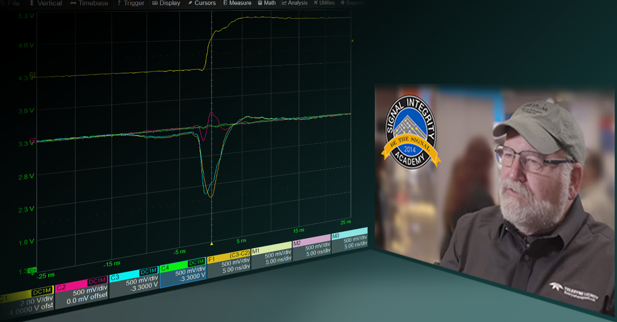
- Measuring the switching noise with an oscilloscope
- Analysis of the results: dos and don’ts to reduce switching noise
Who should attend? Hardware engineers who are responsible for the design of circuit boards with digital components or any test or validation engineer who is concerned about measuring the noise on functioning circuit boards.
What attendees will learn? What is switching noise, how to reduce it and how to measure it using an oscilloscope.
Presented by: Professor Eric Bogatin, University of Colorado and Teledyne LeCroy Fellow